Pinrepair's Clay Harrell's Bible Here
Everything has already been told on sys1, and it is related in the link above.
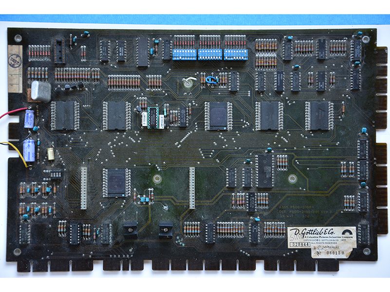
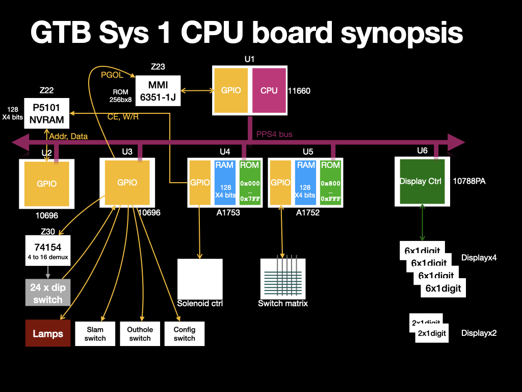
On the figure below is presented a synopsis of the Gottlieb system 1 board. This allows us to identify which device controls which part of the system.

Note that spider chips U4 U5 contain the game operating system ROM. Each of them contains half the content of the CPU board programme. They must be of the same revision. We recently discovered that A1752-CF and u5_cf.bin from MAME have one byte different at address 0x9A. on the other side A1753-CE and u4_ce.bin are strictly identical.
At address 0x00009A: 0x08 0x09
The revision levels that work together are:
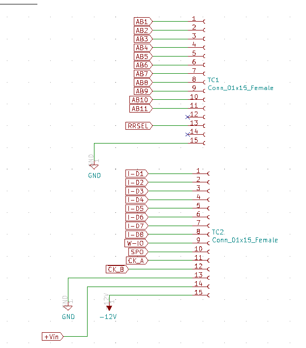
TC1 and TC2 are 2 extension ports. They are used as diag and debug connectors. They collect all signals of the PPS4 system. Address bus, data bus, and control signals. These 2 connectors are of type 1 row x 15 contacts with a pitch of 2.54mm.

U2 is a PPS4 GPIO 10696. 10696 devices have 4 config pins to identify them on the bus. For U2, this is as follows: SC2, SC3: VDD. SC1, SC4: VSS. Or SC2, SC3: -12V (logic 1). SC1, SC4: +5V (logic 0). Therefore, U2 is identified on the bus by b0110 (0x06).
U2 is dedicated to the control of Z22 (P5101L-3), which is the NVRAM of the system. Please note that Z22 is always supplied by the system (batteries).
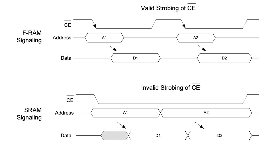
Z22 contains values such as high score, number of games left, etc... P5101L is a specific type of RAM that makes it difficult to find a replacement nowadays. Apart from the sys1, many games that have similar NVRAM solutions (Low power RAM on backup battery with special circuitry for isolating it when necessary and avoiding accidental writes) can be fitted with batteryless replacement parts. For example, one can find them there.
But for GTB system1, as you could see on the site above, there is no such solution. This is because it is more complicated than that. There are 2 reasons:

U3 is a PPS4 GPIO 10696. 10696 devices have 4 config pins to identify them on the bus. For U3, this is as follows: SC1, SC2: VDD. SC3, SC4: VSS. Or SC1, SC2: -12V (logic 1). SC3, SC4: +5V (logic 0). Therefore, U3 is identified on the bus by b0011 (0x03). U3 is dedicated to the conntrol of config DIP-switches, solenoids and CPU controlled light bulbs (through sn74154).
U6 is a PPS4 General Purpose Keyboard and Display interface (GPKD). Its reference number is 10788PA. 10788 is originally a Display and Keyboard interface in standard PPS4 systems. In the GTB System 1 CPU Board, its functionnality is display control only. One could question this fact. For example, why is the switch matrix managed by U5 through GPIOS, and not through a 10788? Probably because the keyboard controller of the 10788 only handles one contact at a time. Simultaneous contacts would not be taken into account properly.
| IOL code | #U | Device Type | Role |
|---|---|---|---|
| b0110 (0x6) | U2 | 10696 | Control P5101 (NVRAM) |
| b0011 (0x3) | U3 | 10696 | Control conf DIP switches |
| b0100 (0x4) | U4 | A1753 | Solenoid control |
| b0010 (0x2) | U5 | A1752 | Switch matrix |
| b1101 (0xD) | U6 | 10788PA | Display control |
The CPU board's principle was to separate the "standard" functions common to all machines from specific functions for a particular model. The CPU Board is equipped with a game PROM, different for each pinball and can be programmed using an advanced language called PGOL (Pinball Game Oriented Language). This invention is the subject of a patent filed in Canada under reference 1‑141‑861.
Invaluable comments about programming in PGOL can be found there.