xxx
PPS4 system is a set of MOS components that allows one to build a programmable system. This set of devices first appeared in 1972. There are 50 instructions. Each of them is 8-bit wide. Data words are 4-bit wide. Some components such as A17xx have capabilities of I/O advanced control. The addition of 2 8-digit decimal numbers takes 240us. Parallel transfer of RAM to I/O is performed in 28us for 4-bit words, or 36us for 8-bit, 56us for 12-bit.
In term of power supply, the PPS4 devices, also called « spider chips » are rather difficult. The supply voltage is [+5V, -12V]. On one hand, this is more than usual. This is too much for standard MOSFETs of nowadays. Modern MOSFETs are often limited to 15V (Vgs, Vds). On the other hand, PPS4 operate in negative logic. A one level corresponds to -12V, while a zero is +5V. VDD = -12V. VSS = +5V. This is an upside down world.
Instead of saying [+5V, -12V], one could have said [0, -17V]. [+5V, -12V] is more usual because PPS4 chips are often talking with TTL devices, that operate at 5V. Thus one has +5V, 0V for feeding TTLs, and +5V, -12V for the PPS4s.
Datasheet (in scanned Pdf) Here
Article wikichip for PPS4 There
Article wikichip for PPS4/2 (evolution of PPS4) There
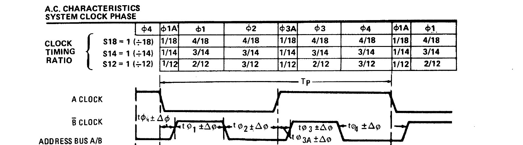
In a PPS4 architecture, every component of the system is synchronized through 2 clock signals named A and /B.
These 2 signals are generated from a parent clock running at 3,579545MHz (this value was chosen because this was the frequency of cheap crystals that were widespread in the 70's. They were installed in every color TV in those times)
3,579545MHz gives us a tick length of about 279ns. A Clock period is made of n ticks, while /B's frequency is twice A's, inverted and delayed by one tick. This delay of one tick is very important, because it determines the four phases of the PPS system. Thus, the 4 in PPS4 (and not the 4 for 4-bit, which is half true).
The value of n is not arbitrary. The recommendation (and generally applied value) is 18. Hence A frequency is around 200KHz and /B is 400KHz. Other standard values for n are 14 (F(A)=256KHz) et 12 (F(A)=298KHz).
The 10706 chip is the original A&/B clock generator from the cheap 3.57MHz crystal. configuration pins select n to 14 or 18. On the PPS4 successors, called PPS4/2, A and /B are internally generated by the micrprocessor (11660 generates A&/B at n=18, while on the version 1 one needed uP 10660 + 10706 for separate clocks generation).
One actually imagines that any value for n is acceptable, as for the 3.57MHz crystal. The only constraint resides in the speed capability of MOS signals. But in theory, max frequency of such an architecture is very high.
There are 21 signals in the PPS4 bus system:
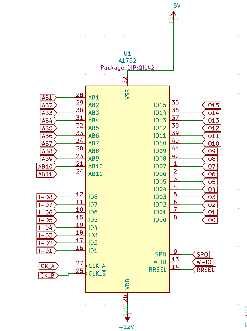
Pinout A17xx
On constate sur ce tableau que le pinout des principaux signaux ne suit pas de logique particulière.