xxx
During the summer of 2019 (Year 1 bc, (before covid)), one of our beloved customers sent us a pinball that was in a very poor condition. They wanted us to refurbish the electronic section. It was a very rare pinball of an Italian brand, called "Bell Games".
This pinball is probably named "Movie" and is actually a Gottlieb's Hulk mod. You can read the story about this Here Besides the original backglass had likely been broken long time ago, and replaced by some ugly "Roger" one.
Pinrepair's Clay Harrell's Bible Here
At first, the repair operation were going beating drums. One just had to read the nice Clay's manual step by step, and change what it needed to be changed. You might have difficulties to find 7448 7-digit chips, but we happen to have a bunch of them here in Vittel. The only problem was to remember where they were hidden in the lab. But it was not time to tidy up. So many things to do and so little time... (This hard to find 7448s gave us the idea of developping a clone version of 10788PAs that integrates all the logic glue including 7448s. This is an ongoigng project at the moment)
So far, so good. But suddenly, trying to fix some targets that were not reacting, we were stuck. That was not looking good at all when we fell here in the manual: "The story ends here"...
The manual was perfectly right at this time. It was very hard, if not impossible, to find a working A17xx. It is even worse if you need a specific version such as an A1752CF. The only way to get one actually is to unsolder one of these jewels by scavenging an original CPU board. You will need to check that it is still good first. Such an in situ checking is not an easy job, unless the entire board is OK. Why would you unsolder such a device if the entire board is working correctly? This is a vicious circle. Hence, if you eventually find a working PPS4 device on the market, there is a high probability that you soon discover that it was a dodgy one.
We refused to give up. Why would not we recreate a device like this? Is not it a very old architecture that would be very easy to copy on these days? Actually there are tons of reasons. The most important reason for going to a solution of emulation instead is that the technical documentation about Rockwell PPS4 components is rather terse. The second other reason why it is madness just imagining to make PPS4 clones, is the power supply voltage. PPS4 are powered through VSS=+5V, VDD=-12V. That is big. This is also a reason why these chips fail very often. The least short circuit on the wrong pins and this is the catastrophe. Moreover, 17V is often to much for the delicate circuits of our 21st century, where voltages are decreasing years after years. 1,2V is a common value today. Then, finding MOSFETs that holds such voltage is not easy, nor cheap.
By these days, there are numerous turnkey solutions of emulation for Gottlieb® system1 CPU boards.
For example:
Janin's board
Nevertheless, we decided to give it a try. We started by studying the original A17xx component The compilation of our findings is available here
At first glance, one might think that emulating a 50-year old PPS4 is not going to be complicated. The cycle for such a device is 200KHz. One might think that using a standard Microchip PIC will make the deal and that's it! Well... Looking at the clock system will rapidly prove the contrary. You will need to detect phases whose duration is about 279ns tick more or less. Using the interruption lines of an MPU would be an utopia in these conditions, even with a powerful one. Hence there is no other choice than to turn oneself towards a charming FPGA.
FPGAs are virtually as fast as you want. Its only Achilles heel resides in its initialization time. Can be hard to manage for hard real-time applications. Fortunately this is not a problem in our case, because in the old times the reset signal could reach 100ms easy! This is enough time for our FPGA to read the tiny bitfield we have. Next question... Which FPGA are we going to choose? Of which brand? We had some good experience with Altera when we were working for RenaultF1 team in 2001-2006. But there was some doubt concerning the dev IDE. Is it still free? Is it still a nightmare with licencing, even though it was free? Because, when developing with FPGAs, time flies by... And then, in the glimpse of an eye, your licence file has expired, and you need to start over, and you don't remember from which site you got it last time, and you don't have time to waste with these things, and bloody hell, let us select something robust. Because yes, these pieces of software are often full of flaws, we don't know why, but this is it.
There were too many questions with Altera, and moreover business evolves rapidly in this field of electronics... Altera is no more Altera exactly, but something related (or drown in) to Intel. Lattice is interesting, but once again you need paid licences to fully get the benefits of Diamond, their Application for programing FPGAs. What do you have eventually? Xilinx? Yes we chose Xilinx, which became AMD in the intervall, which is not necessarily good news. OK, the IDE, whose name is ISE, is not maintained since 2013... It does not work with Windows 11, there are a lot of bugs, it is far from perfect, and should we have to choose again it is not sure if we would go again for Xilinx. But well, this is the cheaper solution when you look at farnell and order the answer by increasing cost. So we went for Xilinx Spartan3 XC3S50 in a QFP100 package (same pinout as XC3S200, if you need more gates) Easy to solder, when you are used to it. Easy to program. Friendly FPGA.
In terms of clock frequency, the minimum requirement is twice the one of the crystal at 3,57Mhz. In prevision of future potential enhancement we went for a quartz at 50MHz. This value is large enough for our needs, and slow enough to be able to manage the PCB layout.
Cloning an A17 device is the most complicated task compared to any other PPS-4 components. Why? Just because A17s contain 3 subsystems and each will use the data bus differently. Which means that all 8 lines of data are bidrirectional. This is the reason why 3 boards are required to achieve the cloning (plus the socket). All other devices of the series may be cloned with only 2 boards.
Please, remember that original spider chips are essentially based on high side P channel MOS transistors. Moreover, they are powered in the range [0V, -17V]. This antique combination of data makes it impossible to find equivalent components. SN7407 for example would not be suitable because they are low side, or any other modern buffer, etc..
This is why the A17 clones are a little bit more expensive, and more complicate.
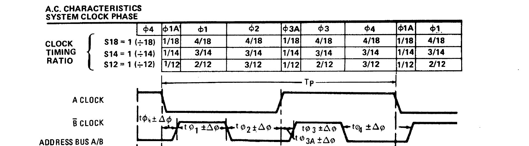
In a PPS4 architecture, every component of the system is synchronized through 2 clock signals named A and /B. This architecture is described here
In VHDL, a specific type is defined to determine in which phase we are for a given slice of time :
type pps4_ph_type is (idlexx, idle00, idle01, idle10, idle11, phi1A, phi1, phi2, phi3A, phi3, phi4); clkgen is defined as a process returning 2 values: pps4_phi is the current clock phase, and diagclk for diagnosing clock signals integrity. clkgen takes 2 signals on input: clk A en clk /B
--hiclk is the 50MHz system clock
--lclk(1) holds the current  A PPS4 clock signal
--lclk(0) holds the current /B PPS4 clock signal
--lclk_prev holds A&/B from the previous hiclk rising edge
--there is no need to filter over more periods, at 50MHz
--because the edges on A and /B are fast enough and
--rising times are always faster than 20ns
--
--
process(hiclk)
begin
	if rising_edge(hiclk) then
		lclk_prev <= lclk;
		lclk(1)<=c_a;
		lclk(0)<=nc_b;
	   if nrst = '0' then
			pps4_t0 <= idlexx;
		else
			case lclk is
				when "00" =>
					if lclk_prev = "10" then
						pps4_t0 <= phi1A;
					elsif lclk_prev = "01" then
						pps4_t0 <= phi2;
					elsif lclk_prev = "00" then
						null;
					else
						pps4_t0 <= idle00;
					end if;
				when "10" =>
					if lclk_prev = "00" then
						pps4_t0 <= phi3A;
					elsif lclk_prev = "11" then
						pps4_t0 <= phi4;
					elsif lclk_prev = "10" then
						null;
					else
						pps4_t0 <= idle10;
					end if;
				when "11" =>
					if lclk_prev = "10" then
						pps4_t0 <= phi3;
					elsif lclk_prev = "11" then
						null;
					else
						pps4_t0 <= idle11;
					end if;
				when "01" =>
					if lclk_prev = "00" then
						pps4_t0 <= phi1;
					elsif lclk_prev = "01" then
						null;
					else
						pps4_t0 <= idle01;
					end if;
				when others =>
					null;
			end case;
		end if; --end if nrst
	end if;

end process;
In the main process, one calls the clock monitoring as follows:
 PHIGN : clkgen port map (hiclk=>SYSCLK, c_a=> not CKA, nc_b=> not nCKB,
                          nrst=>'1', pps4_ph=>pps4_phi, diagclk=>diagAnB);
The diagnostic is performed as follows: For every timeslice of 100ms, the correctness of phase chaining is verified for the last 10 cycles. The precision of timings is not checked. This means that any value for a tick will be accepted, provided that there will be at least 10 cycles running in less than 100ms. Then, a cycle as slow as 10ms will be accepted. Such slow values might be generated for debugging purposes. (The standard cycle period is 5us) The only thing of importance for the diagnostic is actually the sync and phasing of A and /B. The timeslice of 100ms is defined in order to allow for a reset of the diag every 100ms. This will manage for phase locking during reset.
In the current design of our clones, this diag parameter is directly connected to a red flash LED of the Core fpga board. Flashing at 0,5Hz means that clock signals A and /B are present and correctly sync'ed. A faster flash of this LED means that there is a problem on A, /B, or both. No light at all probably means that there is a problem of power supply on the clone.
process(hiclk)
	variable v_diagcycle : natural range 0 to 5000000 := 0;
	variable v_count : natural range 0 to 63 := 0;
begin
	if rising_edge(hiclk) then
		last_pps4 <= pps4_t0;
		v_diagcycle := v_diagcycle + 1;
		if v_diagcycle = 5000000 then
			if v_count < 50 then
				diagclk_t0 <= '0';
			else
				diagclk_t0 <= '1';
			end if;
			v_diagcycle := 0;
			v_count := 0;
		end if;
		if last_pps4 /= pps4_t0 then
			case pps4_t0 is
				when phi1A =>
					if last_pps4 = phi4 then
						v_count := v_count + 1;
					else
						v_count := 0;
					end if;
				when phi1 =>
					if last_pps4 = phi1A then
						v_count := v_count + 1;
					else
						v_count := 0;
					end if;
				when phi2 =>
					if last_pps4 = phi1 then
						v_count := v_count + 1;
					else
						v_count := 0;
					end if;
				when phi3A =>
					if last_pps4 = phi2 then
						v_count := v_count + 1;
					else
						v_count := 0;
					end if;
				when phi3 =>
					if last_pps4 = phi3A then
						v_count := v_count + 1;
					else
						v_count := 0;
					end if;
				when phi4 =>
					if last_pps4 = phi3 then
						v_count := v_count + 1;
					else
						v_count := 0;
					end if;
				when others =>
						v_count := 0;
			end case;
			if v_count > 50 then
				v_count := 50;
			end if;
		end if;


	end if;

end process;
In a PPS4 architecture, there are 2 clock signals A and /B, plus SPO which is the reset signal, and 21 bus signals: A/B1..12, W/IO, I/D1..8. They are described here
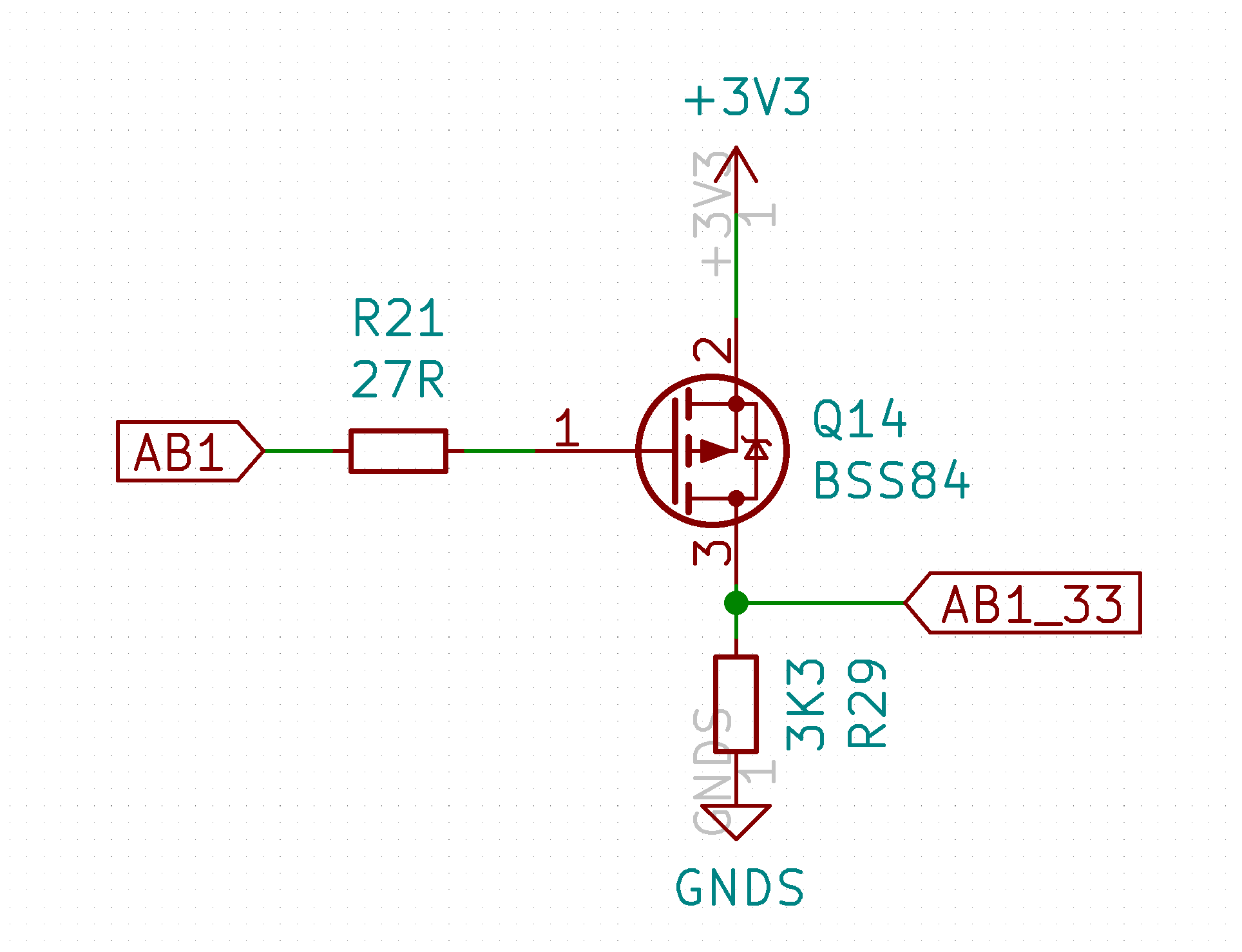
In total, there are 24 input signals to be acquired. Particular attention must be paid to clock signals, whose frequency is the highest in the system (400KHz). A voltage level translation must be applied on each of them, since PPS4 negative logic is [+5V, -12V], whether standard voltage on the fpga is [OV, +3V3]. The standard schematic is displayed on the figure below. It is duplicated 24 times. The gate resistor of 27 Ohms has a 2 reasons: a) protection of the MOSFET and b) limit the current flowing when switching the MOSFET and limit the parasitic oscillations. Can be increased to 100 Ohms Too high values will limit the MOSFET response time. So it is for the drain to ground resistor. The higher the slower, but the lower, the more power consumption it has (current 3.3/3300=>1mA, multiplied by 24 inputs, potentially)
At the beginning of our experimentation on PPS4s, we were not fully confident about our understanding of the data bus. In addition to the voltage translation problematic, there was the question of how to handfle potential unexpected bus contention and hi-Z state. Which bit is dominant? How much current must flow to impose a given state? Conversely, what is the maximum admissible current flowing to or from the bus? etc... We could not take any risk with the unique working CPU board that we had at the time.
Given all these indetermates and the fact that a Spartan3 XC3S50A in VQFP100 has got a lot of I/O pins available, we decided to go for 2 separate 8-bit channels respectively for inputs and outputs. We also thought, at this time, that +5V and HI-Z were all the same, so we neglected to design a gate MOSFET for setting the data bus of the device in HI-Z mode. This will be done in the next PCB design, since we exactly know how it works today.
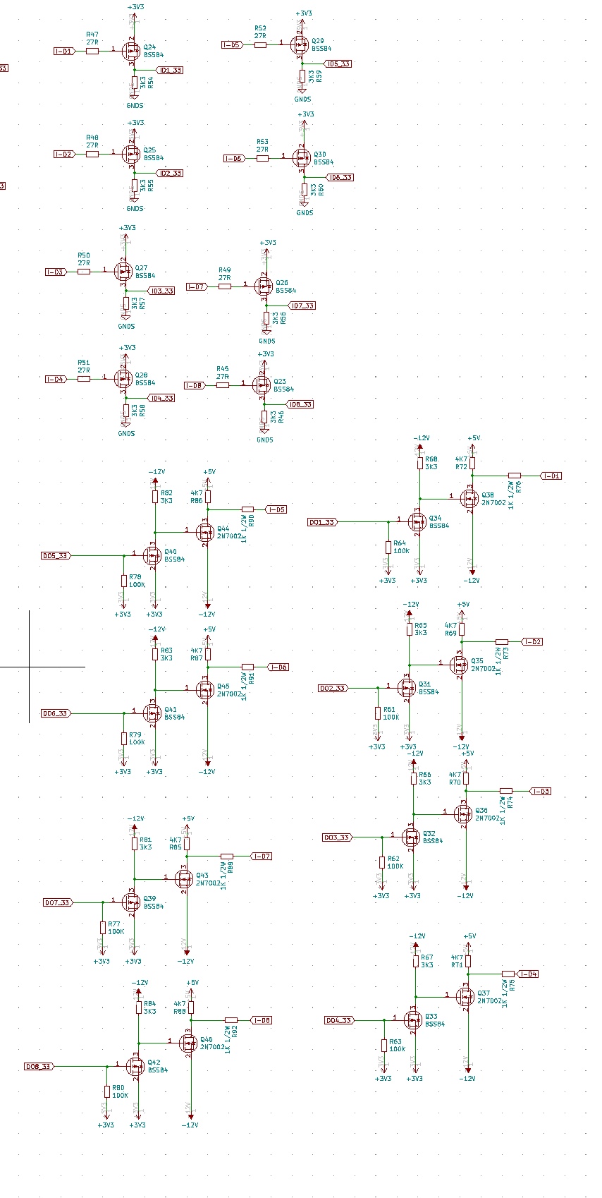
Each *_33 labellized signal is connected to an I/O of the FPGA, through a 100 ohms resistor for protecting the FPGA. In early designs these resistors are not present for PCB surface sparing and fabrication simplicity. Then users must be very careful not to apply an inadvertant overvoltage on these I/Os, because in such an case the FPGA would be destroyed.
The ROM emulation is the easiest job to be achieved. Its size is rather modest : 2K words of 8 bits. We decided to use a simple IP block supplied by Xilinx. It is called IPCore and easy to configure. Please, see the corresponding documentation to get detailled information. The important setup is the .coe file where resides the 2KB ROM binary content in the requested format (see below). Once this IP instance is created and configured, there is only 1 line of VHDL to be inserted:
CFROM : A17INTERNROM PORT MAP (SYSCLK, ROM_Addr_Latch, ROM_DOUT);Then the timing on the bus must be implemented in VHDL and transformed in bitfield for the FPGA. The things to be done:
 process (SYSCLK)
 ...
 begin
   if (rising_edge(SYSCLK)) then
         ...

            last_pps4 <= pps4_phi;

            if last_pps4 /= pps4_phi then

                case pps4_phi is
                    when phi1A =>
                        --nothing to do with ROM in phi1A except for diag
                        ...
                        is_ROM_Device_On <= '0'; --next clock this signal will be unconditionnaly reset
                        if (is_ROM_Device_On = '1') then
                            --diag ROM: check that input=output when we have the control of bus
                            --and that no other source is trying to get the control
                            --also, in mute mode, one can have the clone in parallel
                            --with an original and active device (the one to  be cloned)
                            --Then, one can verify that the clone would deliver the same value
                            --as the original
                            if nDO_int /=  ID then
                                diagbadrom <= '1';
                            end if;
                        end if;
                        --
                        ...

                    when phi1 =>
                        --from beginning of phi1 through end of phi3 device data bus must
                        --be hiz
                        nDO_int <= (others => '0'); --bus data is hiz during phi1 (and also phi3)

                    when phi2 =>
                        --nothing new here, nDO_int still hiz

                    when phi3A =>

                        --A17 samples addr for next rom delivering if we are concerned
                        ROM_Addr_Latch <= AB;
                        --check config bit. Is it us who are selected?
                        if RRSEL = cROMSEL then
                            is_ROM_Device_On <= '1';
                            ROM_used_at_least_once <= '1'; --for diag
                        else
                            is_ROM_Device_On <= '0';
                        end if;

                        ...

                    when phi3 =>
                        --we just have to keep DO in hiz
                        nDO_int <= (others => '0');
                        ...

                    when phi4 =>
                        --A17 push rom data on the bus from begin of phi4 thru end of phi1A
                        if (is_ROM_Device_On = '1') then
                            nDO_int <= ROM_DOUT; -- expose rom values as input of iobufs
                            --this value set continues in phi1A. bus will be deactivated in phi1

                        end if;
                        ...

                    when others =>
                        null;
                end case;
            end if;
        end if;
    end if;
 end process;


CFROM : A17INTERNROM PORT MAP (SYSCLK, ROM_Addr_Latch, ROM_DOUT);
You will find below, the beginning of a .COE file used for the configuration of a XILINX IP ROM block. This will close our discussion about ROM emulation. Thank you for reading up to here.
;******************************************************************
;********  u5_cf ROM Block Memory .COE file  *********
;******************************************************************
memory_initialization_radix=16;
memory_initialization_vector=
81,
77,
1c,
20,
77,
1c,
40,
00,
f2,
77,
1c,
41,
17,
77,
1c,
...
We proceeded in the same way for RAM emulation as we did for ROM, even though it is a bit more complicated for RAM because a RAM access can be a read access, but also a read & simultaneous write command (these 2 operations being performed each on a different nibble). Besides, one does not access the 8 bits of data in the same way as for a ROM access. Finally, there are 2 config bits for the RAM subsystem chip selection, instead of 1 for ROM.
So we started by creating an IP RAM instance from the Xilinx IPCore library. Its size is even smaller than for the ROM section: 128 words of 4 bits.
CFRAM : A17INTERNRAM PORT MAP (SYSCLK, RAM_nRW, RAM_Addr_Latch, RAM_DIN, RAM_DOUT);By these troubled times of supply shortage (as for 2022), it surely would have been wiser to design these ROM and RAM sub-blocks directly in pure VHDL code. That is quite simple, and would have make the entire project independent from the FPGA vendor. It is often said that proprietary IP blocks are tailored to the device for which they are destinated, optimized, more compact, etc... It is probably true, even though we have no problem of real-time nor space, and likely won't have any in our further development. But it is always worth it trying dedicated tools that are offered to you, for free.
Then the timing on the bus must be implemented in VHDL and transformed in bitfield for the FPGA. The things to be done:
        last_pps4 <= pps4_phi;

        if last_pps4 /= pps4_phi then

            case pps4_phi is
                when phi1A =>
                    ...
                    --read RAM addr
                    RAM_Addr_Latch <= AB(7 downto 1);

                        if W_IO = '0' then
                            ...
                            if (RRSEL = cRAMSEL) and (AB(8) = cRAMAB8) then
                                --yes, this is our RAM device
                                is_RAM_Device_On <= '1';
                            else
                                is_RAM_Device_On <= '0';
                            end if;

                        else
                            is_RAM_Device_On <= '0';
                            ...
                        end if;

                    when phi1 =>

                    nDO_int <= (others => '0'); --bus data is hiz during phi1 (and also phi3)

                when phi2 =>

                    --from beginning of phi2 till end of phi3A we have to drive
                    --RAM D1..D4 or I/O D1..D4 or nothing
                    if is_RAM_Device_On = '1' then --RAM selected (during phi1A)
                        nDO_int (4 downto 1) <= RAM_DOUT; --RAM_DOUT is read from CFRAM(RAM_ADDR_Latch)
                        --to be continued in phi3A part dedicated to ram,which means that the only
                        --thing to do is to rest T lines to 1 at the
                        --beginning of phi3. That's very simple in fact.
                    ...
                    end if;

                when phi3A =>
                    --A17 samples addr for next rom delivering
                    ...
                    --RAM device selected? (tested during previous phi1A)
                    if (is_RAM_Device_On = '1') then  --RAM_nRW must be 1 if w_io is also 1
                        --do we have to write to A17's ram?
                        if W_IO = '1' then  --it is a write
                            RAM_DIN <= ID(8 downto 5);
                            RAM_nRW <= "1";   --we will have to reset this signal to 0 the sooner the better
                                              --need to be set for at least 1 or 2 sysclk, (2 to be sure)
                                                    --but 1 should be enough
                                                    --actually we will reset it at the next phi, that will be fine
                        end if;
                        --diag RAM (optional))
                        if nDO_int(4 downto 1) /=   ID(4 downto 1) then
                            diagbadram <= '1';
                        end if;

                        ...
                    end if; --endif of if is_RAM_Device_On else is_IODevice_On
                    is_RAM_Device_On <= '0';
                    ...

                when phi3 =>
                    --we just have to put DO in input mode
                    nDO_int <= (others => '0');
                    RAM_nRW <= "0";

                when phi4 =>
                    ...
                    RAM_nRW <= "0";     --just in case, but it is not necessary

                when others =>
                    null;
            end case;
        end if;
      ...
    end if;
 end process;

CFRAM : A17INTERNRAM PORT MAP (SYSCLK, RAM_nRW, RAM_Addr_Latch, RAM_DIN, RAM_DOUT);
There are 16 pseudo-independent I/Os. We use the term "pseudo" because they are not fully independent. Typically, they are all powered or not at the same time. There is actually a unique command MOSFET which powered all the 16 IOs (5V) when they are configured as output (SOS). Apart from this they are genuinely independent.
Nevertheless, it would not have been sensible to use 16 true port from the FPGA. We decided to make a bus multiplexing of 2x8 bidirectional bits. For the FPGA, we make use of the IOBUF building block (x8: IOx_i_33). Then this bus is connected to 2x74244 for reading inputs (behind 16 input MOSFET), and to 2x74573 for output (before 16 output MOSFET
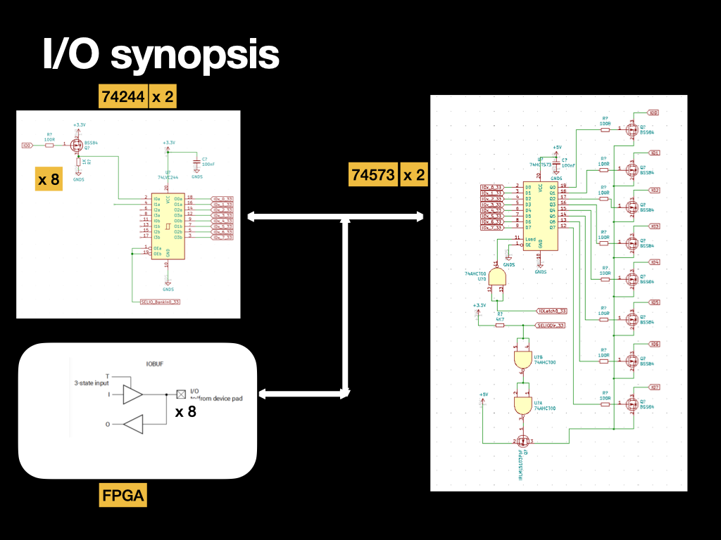
Does it look complicated? Even too complicated? Direct connection to the FPGA is out of the question, for it would require 16 input port pins plus 16 output port pins. Moreover, there is the problem of voltage translation and disabling outputs by program. Then, there is the question of mux or not mux... mux of 2x8bits looks optimum. Finally, the circuit counts 33 MOSFETs, 8 FPGA pins, 2 TTL latches and 2 TTL line buffers.
if last_pps4 /= pps4_phi then

    case pps4_phi is
        when phi1A =>
            ...
            RAM_Addr_Latch <= AB(7 downto 1);
            if W_IO = '0' then
                --all IO devices to be staying off

            else
                --an IO device is called. We will know if it's us
                --by reading rom data value
                if (ID(8 downto 5) = cDEVNUM) then
                    --yes this is our io device id...
                    --get the command from ID1: 0:SES or 1:SOS
                    --command which will be executed at next phi2
                    IOCmd <= ID(1);
                    IONum(3 downto 0) <= AB(4 downto 1);
                    IOBMl <= AB(6 downto 5);
                    is_IODevice_On <= '1';
                end if;
            end if;
--
        when phi1 =>

        when phi2 =>

            if is_RAM_Device_On = '1' then
                ...

            elsif is_IODevice_On = '1' then
                --we are to load accumulator to value of IO(IONum)
                if IOBMl = "00" then
                    --let's activate the reading of IOx(x=IONum)
                    --then, we will assign nDO_int (4) to not this value
                    callloadio <= '1';
                end if;
            end if;

        when phi3A =>
            ...
            --RAM device selected? (tested during previous phi1A)
            if (is_RAM_Device_On = '1') then  --RAM_nRW must be 1 if w_io is also 1
                ...
            elsif is_IODevice_On = '1' then
                --lets read the accumulator from DO8
                --to get the param
                --IOCmd contains ses or sos
                if IOCmd = cSES then -- cste cSES set at 0 which is
                    --D04=1 :  enable all outputs
                    --DO4=0 : disable all outputs ==> all Ts configured as input (T=1)
                    --(T=0: outputs, T=1: inputs)
                    --CtrlIODIR=1: IOs as input, CtrlIODIR=0: IOs as output
                    if ID(8) = '0' then --set IOs as outputs
                        --That means : set IOs as output if out from fpga=1
                        --When fpga out is 0, out mosfet is off then we shall be in input mode
                        --in order to catch the state of the pin coming from the outside
                        --Thus, we have to set T(x)<=0 if OIO_VEC=1 and T(x)<=1 otherwise
                        SELIODir <= '0';    --allio are input at reset. 0 is output, 1 is input
                    else
                        --disable all outputs
                        SELIODir <= '1';    --allio are input at reset. 0 is output, 1 is input
                    end if;
                else
                    --cSOS
                    if IOBMl = "00" then

                        -- IOx_out <=  not ID(8);  -- obsolete old hw
                        iomem := unsigned(IIO_MEM);
                        iomem(to_integer(unsigned(IONum))) := not ID(8);
                        IIO_MEM <= std_logic_vector(iomem);
                        --we need to initiate the latching (2 cycles at 50MHz should be enough)
                        --signal will be reset after counting 2 clock cycles
                        IOLatchSig(1) <= not IONum(3);
                        IOLatchSig(0) <= IONum(3);
                   TIO_ENABLE_SIG <= '0'; --set IOs internally as outputs
                        if IONum(3) = '1' then
                            IIO_VEC <= std_logic_vector(iomem(15 downto 8));
                        else
                            IIO_VEC <= std_logic_vector(iomem(7 downto 0));
                        end if;
                    end if;
                end if; --endif of if cSES
            end if; --endif of if is_RAM_Device_On else is_IODevice_On


        when phi3 =>
                ...
        when others =>
            null;

--state machine
--
--
if (rising_edge(SYSCLK)) then
    --start of latch management of IO on write
    --IOLatch is maintained to 1 for 2 clock cycles
    if IOLatchSig /= "11" then
        IOLatchTime := IOLatchTime +1;
        if IOLatchTime = 4 then
            IOLatchTime := 0;
             IOLatchSig <= "11";
            TIO_ENABLE_SIG <= '1';  --set internal IOs as inputs (IOx bus)
        end if;
    end if;
    --end of latch management of IO on write

    --start of IO reading
    if callloadio = '1' then
        callloadio <= '0'; --this is a state machine
        callreadio <= '1';
        --disable latches
        IOLatchSig <= "11";
        --set T sig of fpga in read mode
        TIO_ENABLE_SIG <= '1'; --set IOs internally as input
        if IONum(3) = '1' then
            IOSelSig <= "01";   --activate IO8..15 bank
        else
            IOSelSig <= "10";   --activate IO0..7 bank
        end if;
    end if;
    if callreadio = '1' then
        callclrdio <= '1';
        callreadio <= '0'; --this is a state machine. reset
        --final step. We assign the accumulator with the right value
        nDO_int (4) <= not OIO_VEC(to_integer(unsigned(IONum(2 downto 0))));
    end if;
    if callclrdio = '1' then
        IOrdTime := IOrdTime +1;
        if IOrdTime = 4 then
            IOrdTime := 0;
             callclrdio <= '0';

            --final step. We close enble sig
            IOSelSig <= "11";   --deactivate IO0..7 bank
            end if;
    end if;

    --end of IO reading
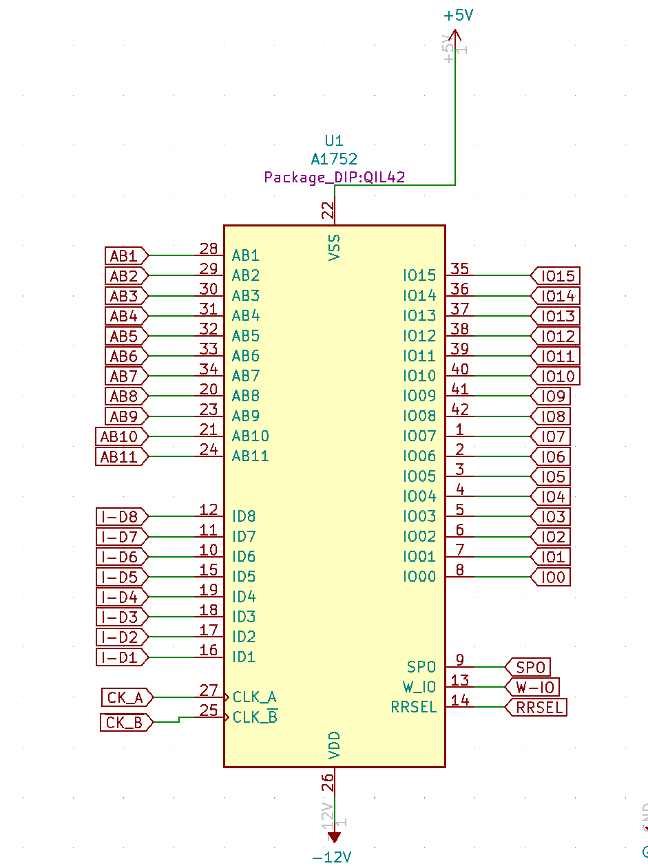
Pinout A17xx
An additional feature in the PPS-4/2 CPU is an expanded discrete output capability. This capability is achieved by using the same instruction (DOA) as in the PPS-4 CPU but providing more I/O control. In the PPS-4 the DOA instruction causes the contents of the accumulator (A) to be transferred to an output buffer and then retained until another DOA instruction is executed. The contents of this buffer controls the output drivers. In the PPS-4/2 CPU this same function is performed but, additionally, the contents of the X register are transferred to a similar second set of buffers and drivers (DIO) so that the DOA instruction causes 8 bits to be available to external devices.
On constate sur ce tableau que le pinout des principaux signaux ne suit pas de logique particulière.