xxx
The context is as follows: One wants to read the content of programme which resides in both A175x of the GTB CPU board. The first half of the programme resides in U4, A1753-xx. The second half is in U5, A1752-yy. For each A175x, the objective is to read the 2048 bytes of ROM contained in it, without unsoldering the component from the GTB SYS1 CPU board.
To do so we need to inactivate the CPU, because we don't want the system to execute read data, while acquiring it. TC3 can be used to achieve this.
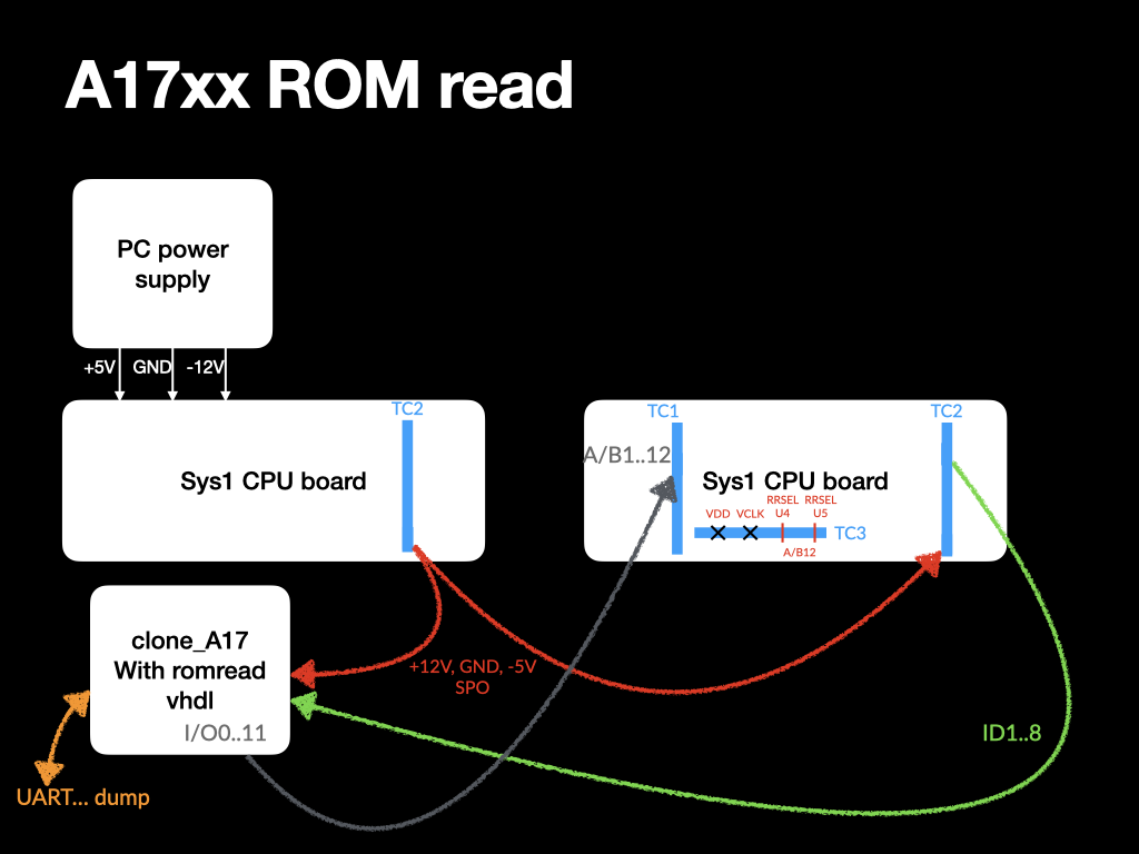
As you can see on the figure above, we use 2 cpu boards. The purpose of the first one is to provide the power supply (+5V, -12V, GND) and reset (SPO) and clock signals (CLK A & CLK /B) to the rest of the system, namely the second cpu board which holds the 2 A17s to be read, and our clone_A17 which will be used to generate the successive addresses for the complete reading of the devices.
But, the first thing to achieve is to disable the main processor U1 (11660CF). Otherwise, we would be facing the problem that U1 would try to execute any seen ROM byte on the data bus, as it is its regular task. Then, incrementing the PC to access the next byte would be impossible and clash with the addresses set by U1 itself. This is also why we need 2 GTB Sys1 boards, because by deactivating U1 on the board under examination, we also stop the clocks A and /B. As we need A and /B clock in order to access the A17s, either we make it from our clone, or we simply pick it from a vaguely operational SYS1 board. The second option is simpler, for generating clocks at such frequency is not easy to achieve with our clones (due to the laziness of output MOSFETs when you have hign drain impedance in order to limit current consumption, as we always do since there are a lot of MOSFETs in parallel.
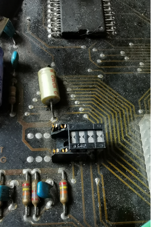
And we are lucky because the conceptors of the GTB SYS1 have foreseen this need. Thanks to TC3, you can disable U1 (VCLK) by disconnecting the 2 first connections of TC3. Take care to keep the 2 other connections that are required for directing A/B12 to RRSEL of each A17xx. (see picture of PCB above).
Our clone is equipped with a specifically designed bitfield. This programme has an UART for launching the action of reading, verifying, selecting the A1752 or the A1753, etc... and for uploading the result of reading. The bitfield also contains the required vhdl for generating the consecutive addresses A/B1..A/B11, plus RRSEL in sync with clocks, that are sent to the device to be read. Finally, I/D1..8 is collected in a special internal diagnostic RAM, which can be sent on a computer through the UART, when it's complete.